Consulting . Research . Outsourcing . Technology
Nanoelectronics and Its Industrial Applications Program
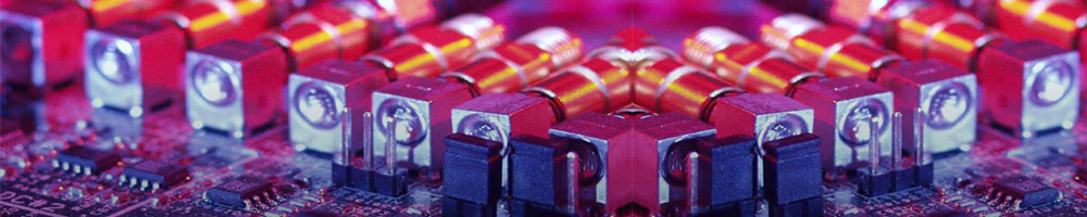
Nano Scale ElectronicsNanotechnology is continually playing vital role to improve the capability of electronic products. The technology also made the devices very light making the product easy to carry or move and at the same time it has reduced the power requirement. LCD and its improved versions are example. The quality of display screens has improved a lot while its size became very thick, decreased weight and reduced power consumption Nanotechnology has made size of memory chip very small but storage capacity up to 1 terabyte per square inch. It has been reduced like a circuit where all the power can be stored. Ever since the use of nano scale technology have implemented in the process of manufacturing electronic products it has brought a revolution in this industry. |
|||||||||||||
|---|---|---|---|---|---|---|---|---|---|---|---|---|---|
Program OverviewFor the budding engineers and professionals it is very important to know and understand the latest that when they join the industry they are capable of giving back to the industry what they have learned and gained during their academic pursuits. Currently Science & Technology based research has been transformed because of inventions and innovations been made in the field of visualizations, characterization, synthesis, materials & ability to commercially manufacture at 10-9 m scale level.At the dimension of 10-9 m ( billionth of a meter ) the ability to create new and wonderful products and materials gets a tremendous boost, this is because at this scale we have the ability to work at atomic or molecular level and thus able to create things which are remarkably significant to current comparisons. The Program Nanoelectronics & Its Industrial Applications an advanced program meant to enhance the knowledge base of participants in the area of electronics. It enables the participant to be able to understand the various processes and business aspects of nano scale technology in electronics from the point of view of the industry. The program comprises of nine modules. The modules include online tutorials and assessments, and are evaluated through project work and online assignments. The program consists of two online mid-term assignments, a final online examination and project work. The mid-term assignments contribute 20% to the final marking. The final online examination contributes 30%, and the project work makes up 50% of the final marks. Program Aim The innovative Program - Nanoelectronics & Its Industrial Applications aims to give participants a thorough grounding in the skills necessary for a technology-based career in industries. The course covers technologies used to design, realize and analyze micro and nano-scale electronic devices, materials and systems, coupled with general and technology management. This is supported by project work and ensures the graduates to emerge training in a wide range of technical and management skills, and have a sharp appreciation of the relevance of the subject to industrial needs. Learning Outcomes of the Program Program Outcome Successful students will secure positions in the newly developing Nano scale systems and technology-based electronic industries as well as more traditional industries, such as microelectronics and precision engineering. Graduates will be able to pursue careers in a diverse range of electronics industries. Program Delivery MethodologyNanoelectronics & Its Industrial Application Program- Distance Participation has a unique delivery methodology. The program delivery is through regular dispatch of training kit (study material), eLearning user id & password and Multimedia CD. The program support is provided through chat/e-mail / telephone / web portal. Participant’s Role Submission of complete application form and necessary program fee in the form of demand draft drawn in favors of "Nano Science and Technology Consortium" payable at Delhi/New Delhi to the organization NSTC’s Role Support Material and Confirmation Letter are dispatched to the participant. Dispatch is made within 10 days after receiving the application form and program fee. Fee Structure and Payment NormsThe program fee should be sent along with duly completed application form. The fee should be paid through a Demand Draft/ at par cheque, issued in favor of Nano Science and Technology Consortium payable at Delhi/ New Delhi.
* Fee inclusive of Service Tax, which is subject to be changed Nano Science and Technology Consortium
A-118 First Floor, Sector-63 |
|||||||||||||